
Antiferromagnets are remarkable materials that possess unique magnetic properties characterized by the antiparallel alignment of neighboring atomic magnetic moments. This arrangement results in the cancellation of the overall magnetization, leaving the material without a detectable magnetic field. Such properties have significant implications for burgeoning fields like spintronics and electronic device development. Researchers are increasingly interested in how these materials can be utilized in innovative technologies, making recent discoveries in this area particularly exciting.
A groundbreaking study conducted by a team at Harvard University has shed light on the antiferromagnetic diode effect observed in MnBi2Te4, a material distinguished by its centrosymmetric crystal structure. Unlike typical diodes, which exhibit a directional current flow, this effect appears in a material that doesn’t have a clear mechanism for directional charge separation. The implications of this research, published in *Nature Electronics*, open up potential pathways for the advanced design of electronic components, including in-plane field-effect transistors and devices capable of harvesting microwave energy.
The diode effect has been documented across various materials, with applications extending to radio receivers, digital circuits, and sensors. This recent revelation that an antiferromagnetic material can demonstrate diode behavior expands the landscape of potential applications and benefits in electronic systems.
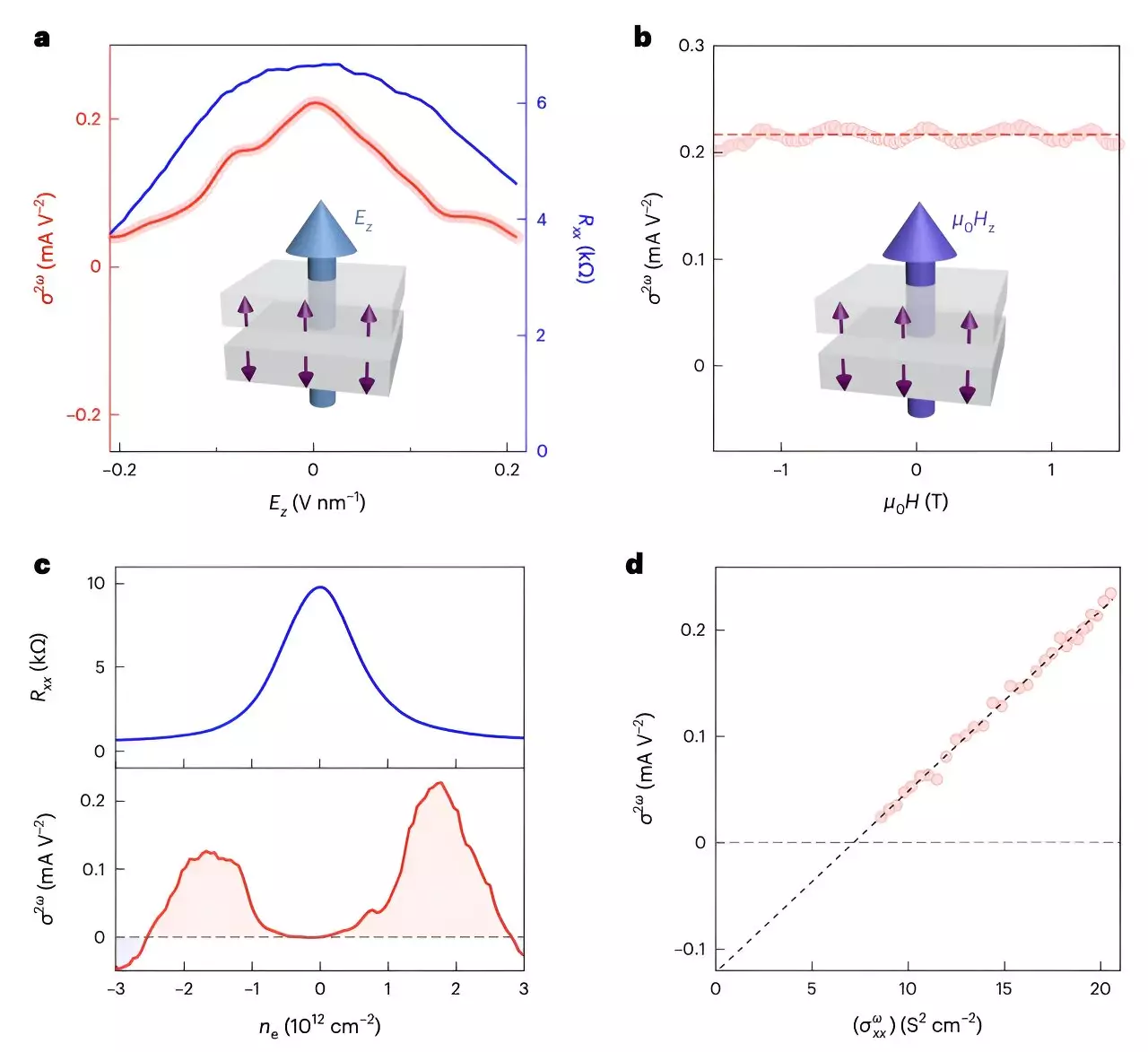
The Harvard researchers engineered devices from even-layered MnBi2Te4, applying two distinctive configurations for their electrodes: Hall bar electrodes and radially arranged electrodes. Through these configurations, they successfully witnessed nonlinear electrical transport, a hallmark of the antiferromagnetic diode effect.
To validate their findings, the research team employed an array of sophisticated analytical techniques. Among these was a spatially resolved optical method alongside electrical measurements for sum frequency generation (SFG). Their results illuminated significant nonlinear phenomena associated with second-harmonic transport within the material, showcasing the ability to engineer devices that exhibit extraordinary electronic characteristics.
The potential applications of the antiferromagnetic diode effect are both diverse and promising. The researchers highlighted its utility in developing antiferromagnetic logic circuits, which could revolutionize how data is processed and stored within electronic devices. Furthermore, the integration of these materials into microwave harvester technologies could lead to more efficient energy capture systems, addressing the growing need for sustainable energy solutions in a technologically driven world.
The team’s findings suggest that the electrical sum-frequency generation technique could be pivotal in detecting nonlinear responses in quantum materials, potentially paving the way for new experiments and applications in material science.
The work undertaken by the Harvard team represents a significant advancement in understanding and harnessing antiferromagnetic materials. By demonstrating an antiferromagnetic diode effect in a centrosymmetric crystal, they have opened avenues for further investigation and application in various technological realms.
As researchers delve deeper into this phenomenon, the possibilities for creating next-generation spintronic devices that leverage the unique properties of antiferromagnetic materials seem highly promising. This research not only pushes the boundaries of current understandings of material science but also presents a critical stepping stone toward the development of smart, efficient, and sustainable electronic technologies in the future.
Through continued exploration and innovation, the integration of antiferromagnetic characteristics into practical device applications could redefine the landscape of electronics and contribute to solving some of the most pressing challenges in technology today.
Leave a Reply