
In a groundbreaking achievement, researchers at UC Santa Barbara have successfully engineered the inaugural “movie” that captures the transit of electric charges across the boundary of two diverse semiconductor materials. Utilizing the advanced scanning ultrafast electron microscopy (SUEM) methods spearheaded by Bolin Liao’s laboratory, this team has for the first time visually documented the transient and elusive behavior of photocarriers in these materials. Liao, an associate professor specializing in mechanical engineering, emphasized the significance of this development, stating, “Many theoretical models exist, but observation has remained elusive. Our visualization brings a fresh perspective to these established theories.”
Published in the esteemed Proceedings of the National Academy of Sciences, this research can significantly influence future advancements in semiconductor technology. Traditional textbooks have expounded on the theoretical aspects of charge transport in semiconductors, providing indirect measurements but lacking direct observational evidence. The visualization of charge movement will enable materials scientists to critically evaluate established theories and potentially refine them using empirical data.
Photocarriers, formed when light energy interacts with semiconductor materials, are a fundamental element in the performance of devices like solar cells. Here, sunlight excites electrons within the semiconductor, enabling their movement and resulting in the generation of electrical current. However, this process is not without its flaws; the majority of these photocarriers dissipate their energy as waste heat almost instantaneously—in picoseconds—leaving only a small fraction of energy available for harnessing in traditional photovoltaic applications.
Understanding this phenomenon is crucial, as the ‘hot’ state of photocarriers contains considerable energy that could enhance energy efficiency. Yet, the challenges this state presents, such as the heat that may compromise device performance, are also significant. Therefore, comprehending the dynamics of these hot carriers, especially at the critical interface between different semiconductor materials—termed the heterojunction—is essential for advancing technologies such as lasers, sensors, and photocatalytic systems.
Liao’s research team zeroed in on the heterojunction formed by silicon and germanium, two common semiconductor materials recognized for their potential in a myriad of applications including photovoltaic systems and telecommunication technologies. Collaborating closely with researchers from UCLA, they explored how these materials interact at their junction.
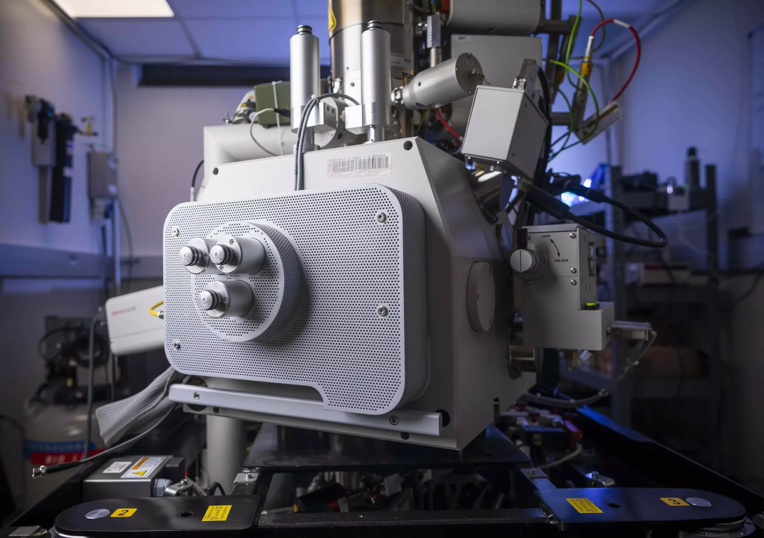
The innovative imaging technique hinges on a unique methodology: employing ultrafast laser pulses that act like a shutter to capture events occurring over picosecond to nanosecond timescales. According to Liao, this method opens profound new avenues for capturing dynamic events that were previously too swift to observe. “The ramifications of our findings extend well beyond mere observation; they serve as a window into the microscopic processes happening within these semiconductor devices,” Liao remarked.
The visualizations produced during this research revealed vital insights into the behavior of hot photocarriers. When excited within uniform regions of silicon or germanium, these carriers exhibit remarkable speeds attributed to their elevated thermal energy. Yet, the dynamics change drastically at the heterojunction—some of the carriers become trapped by the junction’s potential, leading to a marked reduction in mobility.
This critical trapping effect directly correlates with the efficiency of devices that rely on the effective separation and utilization of these charges. Although semiconductor theory has long acknowledged these trapping phenomena, the ability to observe them effectively introduces a new layer of understanding. Liao expressed astonishment at achieving direct imaging of such effects, a revelation that may shift how semiconductor device engineers approach design challenges.
This pioneering capability to visualize photocarrier behavior at heterojunctions is a significant step forward in semiconductor research at UC Santa Barbara, an institution notable for its contributions to the field. The work recalls the legacy of Herb Kroemer, whose revolutionary ideas about heterostructures in semiconductors in the late 1950s laid the foundation for the modern semiconductor industry. His assertion that “the interface is the device” has become instrumental in shaping the landscape of information technology today.
As semiconductor technology continues to evolve and integrate into various applications, from computers to renewable energy arenas, the findings from Liao’s team will undoubtedly fuel further inquiries into enhancing the efficiency and capability of these critical materials. The journey, while filled with complexities, holds the promise of unlocking unprecedented advancements in the world of electronics and energy.
Leave a Reply