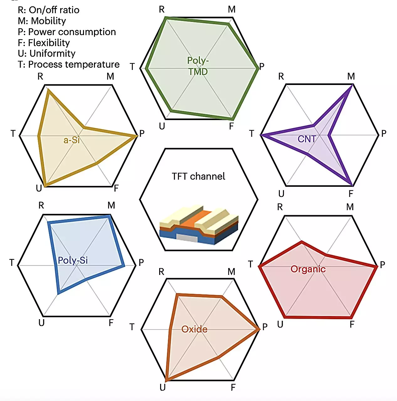
Electronic engineers have been pushing the boundaries of transistor design in recent years, with a focus on creating smaller and more efficient transistors. Traditional silicon-based field effect transistors (FETs) have limitations when it comes to scaling down to smaller sizes. This has led to the exploration of alternative designs using materials such as Transition Metal Dichalcogenides (TMDs) with higher electron mobility.
One of the most promising materials for scalable FETs is molybdenum disulfide (MoS2). This compound, made up of molybdenum and sulfide atoms in a 1:2 ratio, has shown great potential in the development of smaller and flexible devices. Researchers at the Samsung Advanced Institute of Technology (SAIT) and Seoul National University recently demonstrated the integration of MoS2 transistors on a 200 mm wafer, showcasing the scalability of transistors based on this material.
Fabrication and Performance
The team of researchers utilized metal-organic chemical vapor deposition (MOCVD) to fabricate large-scale arrays of MoS2 FETs. By eliminating the Schottky barrier at the interface between the MoS2 material and metal, they were able to enhance the FETs’ carrier mobility. This fabrication strategy proved to be compatible with current electronics manufacturing processes, with a remarkable yield of over 99.9%.
The FETs designed and fabricated by the research team displayed promising results in initial tests, outperforming previously introduced FETs based on MoS2 in terms of field-effect mobility, contact resistance, and on-current densities. The team attributed this success to the innovative fabrication steps they introduced, which focused on eliminating the Schottky barrier and reducing contact resistance. By identifying factors that could impact performance and yield, such as impurities on the contact and material peeling, the researchers demonstrated the feasibility of reliably fabricating MoS2 FETs at existing industrial facilities.
Future Prospects
The integration of MoS2 FETs on a 200 mm wafer highlighted their uniformity and potential for large-scale commercialization. This study opens up opportunities for other research teams to explore similar FET designs and fabrication processes. By continuing to innovate in the field of two-dimensional semiconductor transistors, advancements in technology can be made to facilitate the development of highly performing transistors based on materials like MoS2.


Leave a Reply