
Metal halide perovskites have emerged as a highly promising class of materials for the development of thin-film transistors due to their remarkable optoelectronic properties. In recent studies, researchers have achieved significant success in using tin (Sn) halide perovskites to fabricate high-performance p-type transistors with impressive field-effect hole mobilities. However, the challenge lies in developing n-type transistors with comparable performance, which is crucial for the realization of complementary logic circuits. To address this gap, scientists have been exploring the potential of lead halide perovskites for designing n-type transistors, leading to groundbreaking advancements in the field.
Lead halide perovskites have traditionally suffered from ionic defects that restrict the electron mobilities of resulting transistors. However, a pioneering strategy introduced by researchers from institutions such as the National Centre for Scientific Research Demokritos and École Polytechnique Fédérale de Lausanne (EPFL) has revolutionized the scenario. By leveraging formamidinium lead iodide (FAPbI3) perovskite and incorporating innovative techniques, they have successfully demonstrated n-type transistors with field-effect mobilities of up to 33 cm2 V−1 s−1, marking a significant milestone in the field of optoelectronics.
One of the key factors that enabled the researchers to achieve such remarkable results was the utilization of a methylammonium chloride (MACI) additive. This additive played a crucial role in regulating the strain in FAPbI3, thereby enhancing its properties and optimizing its performance characteristics. By employing a comprehensive approach that encompassed strain relaxation and the suppression of undercoordinated lead, the team was able to stabilize the perovskite lattice, improve surface morphology, enhance crystallinity and orientation, and establish low-defect perovskite–dielectric interfaces. These advancements were instrumental in elevating the performance of the n-type transistors to unprecedented levels.
Future Implications and Applications
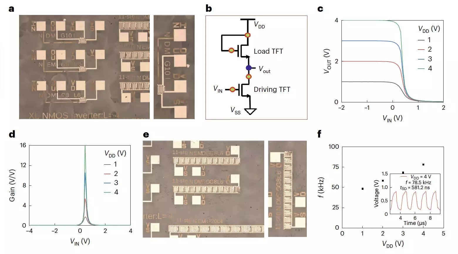
In their experimental evaluations, the researchers observed highly promising outcomes, including superior electron mobilities, negligible hysteresis, and exceptional operational stability even under challenging bias stress conditions. Furthermore, the team successfully utilized these transistors to fabricate all-perovskite unipolar inverters and 11-stage ring oscillators, showcasing the versatility and applicability of their approach. Looking ahead, this innovative fabrication strategy holds immense potential for revolutionizing the landscape of integrated circuits containing metal halide perovskite transistors, paving the way for the development of high-performance and cost-effective electronic devices. As these n-type transistors undergo further testing and integration into various electronic applications, the possibilities for innovation and advancement in the field of optoelectronics are truly limitless.
Leave a Reply