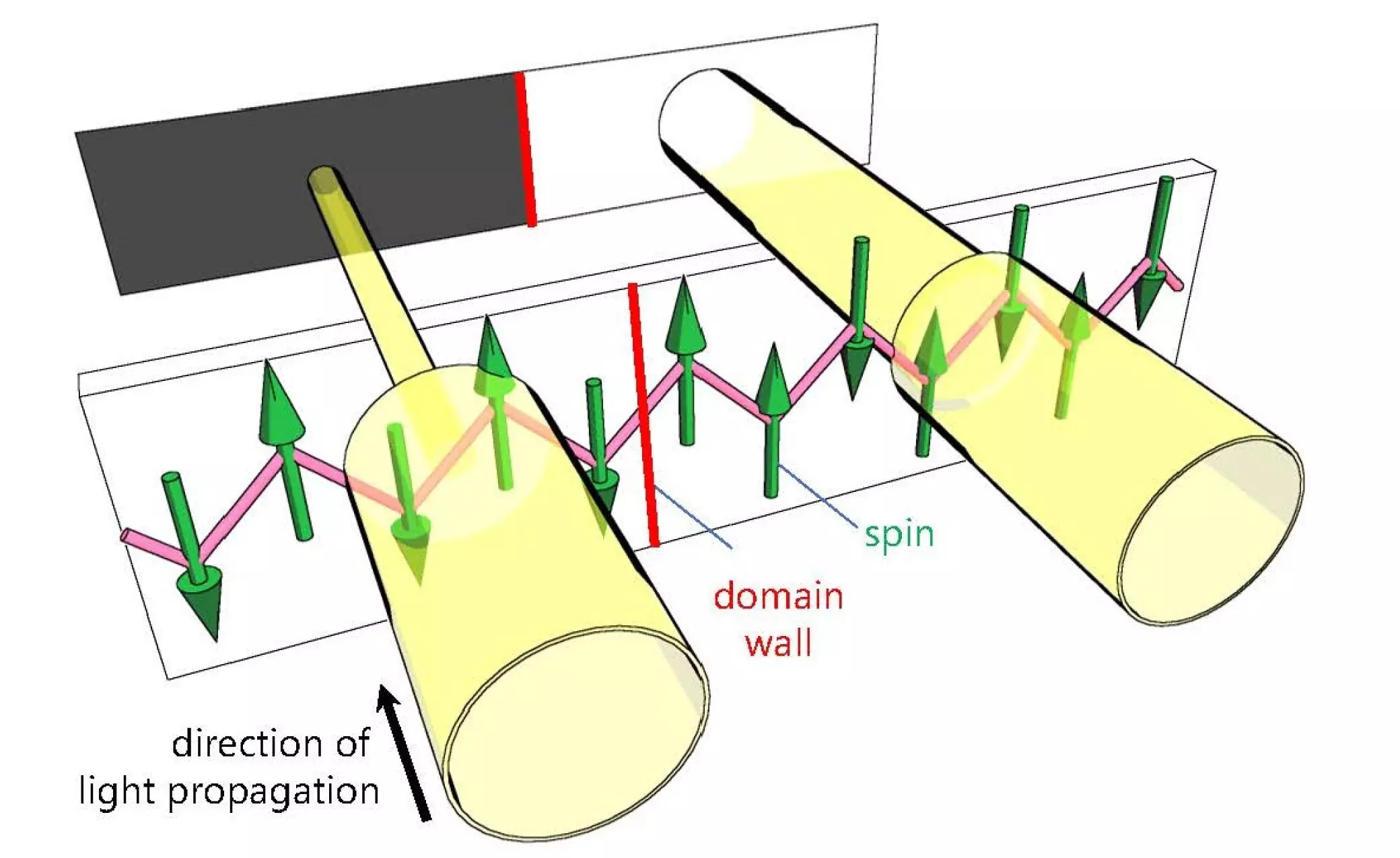
In the realm of physics, certain materials possess captivating properties that often challenge our traditional understanding. Among these, antiferromagnetic materials stand out not only for their unique magnetic characteristics but also for their potential applications in advanced technology. A recent breakthrough by researchers from Osaka Metropolitan University and the University of Tokyo sheds light on these enigmatic materials, revealing methods to visualize and manipulate their intricate magnetic domains using light and electric fields. Their innovative work, highlighted in Physical Review Letters, signals a promising step forward in the exploration of quantum phenomena.
Understanding Antiferromagnetism
Before delving into the nuances of this discovery, it is crucial to comprehend what antiferromagnetic materials are. Unlike their ferromagnetic counterparts, which have aligned magnetic spins creating strong north and south poles, antiferromagnetic materials are characterized by a unique arrangement where neighboring spins point in opposite directions. This cancellation results in an absence of a net magnetic field, rendering them non-magnetic in conventional terms. Researchers are particularly interested in quasi-one-dimensional antiferromagnets, where the magnetic behavior is primarily confined to linear chains of atoms. These materials possess untapped potential for next-generation technologies, including electronics and memory devices, due to their distinct magnetic properties.
Studying antiferromagnets presents significant challenges, primarily due to their low magnetic transition temperatures and diminutive magnetic moments. The observation of magnetic domains—small regions where atomic spins align—has traditionally been hampered by these factors. Kenta Kimura, an associate professor and lead author of the study, articulated these challenges, stating that visualizing magnetic domains has proven particularly complex. Boundary regions between domains, known as domain walls, further complicate the analysis of these intricate materials.
An Innovative Approach to Visualization
To confront these observational hurdles, the research team employed an innovative technique involving nonreciprocal directional dichroism. This sophisticated phenomenon allows for the detection of light absorption changes in a material based on the direction of light and its magnetic characteristics. By applying this principle to the antiferromagnet BaCu2Si2O7, the researchers successfully visualized its magnetic domains and illuminated the coexistence of opposing domains within the crystal structure. The revelation that these domains align along precise atomic chains represents a significant advancement in the comprehension of quantum materials.
One of the most exciting aspects of the study is the demonstration of magnetic domain manipulation through an electric field, enabled by magnetoelectric coupling. This interplay between magnetic and electric properties allows for the movement of domain walls while preserving their original orientation. Kimura expressed enthusiasm regarding the implications of such a straightforward and swift optical microscopy method, which could pave the way for real-time visualizations of dynamic domain walls. The ability to manipulate these walls at a quantum level may unleash new avenues for research and technological innovation.
Implications for Future Technologies
The insights garnered from this research not only advance our understanding of quantum antiferromagnets but also hint at broader applications. The potential to apply this observational method to diverse quasi-one-dimensional antiferromagnetic materials could significantly enhance our knowledge of how quantum fluctuations influence magnetic domain behavior. This could ultimately aid in the design and development of cutting-edge electronics, leveraging the properties of antiferromagnetic materials for practical applications.
The recent achievements in visualizing and manipulating magnetic domains within quantum materials signify a landmark moment in physics and materials science. By unraveling the complexities of antiferromagnetic behavior and harnessing innovative observation techniques, researchers are crafting a pathway toward future quantum devices. As we continue to probe deeper into the enigmatic world of quantum materials, the potential for groundbreaking advancements in technology becomes increasingly tangible. With each new discovery, we edge closer to a future where the unique properties of antiferromagnetic materials can be transformed into practical innovations, reshaping our technological landscape.


Leave a Reply