
The integration of two-dimensional (2D) semiconducting materials into electronic components has been a challenging task due to the difficulty of optimally interfacing these materials with gate dielectrics. The presence of interfacial traps often leads to rapid performance degradation in transistors, hindering their potential advantages over bulk semiconductors.
Researchers at King Abdullah University of Science and Technology (KAUST), Soochow University, and other institutes worldwide have recently introduced a groundbreaking approach to address this issue. Their proposed design, detailed in a paper published in Nature Electronics, revolves around the use of hexagonal boron nitride (h-BN) dielectrics and metal gate electrodes with a high cohesive energy.
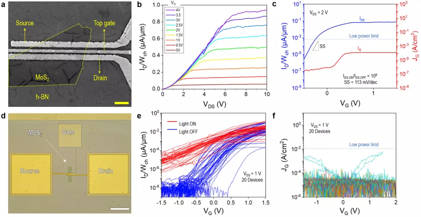
The research team discovered that utilizing platinum (Pt) as an anode in conjunction with h-BN significantly reduces the likelihood of dielectric breakdown. Comparing Pt/h-BN gate stacks to Au/h-BN gate stacks, the former exhibited a 500-fold decrease in leakage current and demonstrated a high dielectric strength of at least 25 MV/cm. This observation led to the exploration of chemical vapor deposited h-BN as a promising gate dielectric material for 2D transistors.
The team successfully fabricated over 1,000 devices utilizing chemical vapor deposited h-BN as dielectrics. By incorporating high cohesive energy metals like Pt and tungsten (W), they achieved improved compatibility and performance. The vertical Pt/h-BN/MoS2 transistor structure proved to be highly reliable, with a clean van der Waals interface between MoS2 and h-BN enhancing gate control and minimizing defects.
Contrary to common belief, the research team demonstrated that selecting the right metal electrodes enables the effective use of CVD h-BN as a gate dielectric in field-effect transistors with MoS2 channels. The integration of high cohesive energy metals like Pt and W led to a significant reduction in leakage current across h-BN dielectrics, paving the way for the development of highly performing 2D semiconductor-based devices.
The recent breakthrough in fabricating 2D semiconductor-based transistors offers promising prospects for reducing current leakage and achieving high dielectric strength. The potential applications of this research extend to the fabrication of reliable solid-state microelectronic circuits and devices, with the possibility of advancing Moore’s Law through the development of ultra-small, fully 2D transistors.
The innovative approach presented by Shen and her colleagues marks a significant milestone in the advancement of 2D transistors. Their findings have the potential to revolutionize electronic component development, opening up new possibilities for the utilization of 2D semiconducting materials in next-generation technologies.
Leave a Reply