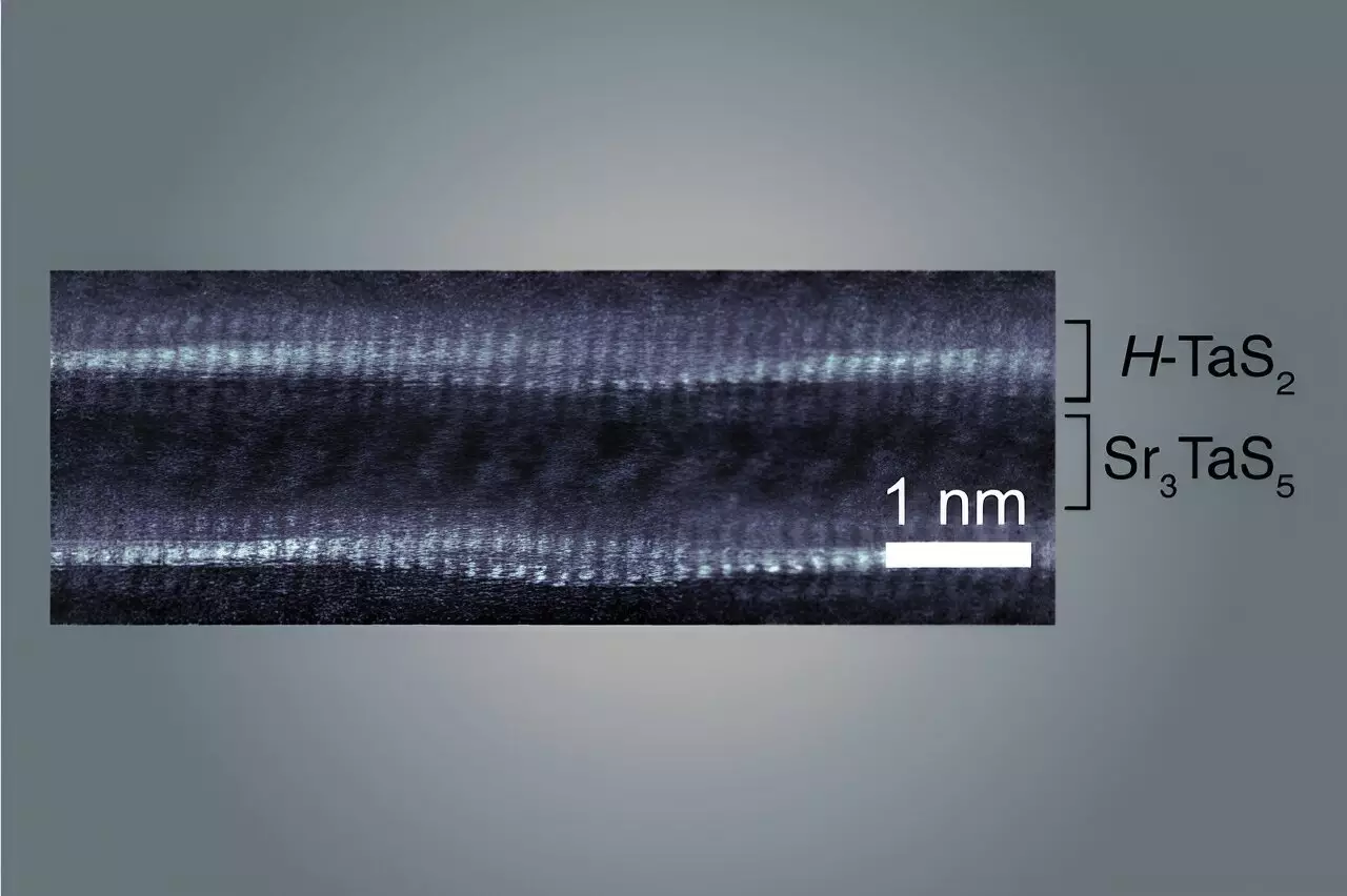
The realm of superconductivity—a state in which materials conduct electricity with zero resistance—has long intrigued physicists and engineers. Recently, a collaborative effort led by physicists from MIT has pushed the boundaries of this field by unveiling a novel material featuring exceptional superconducting and metallic traits. What sets this discovery apart is not merely the functionality of the material itself but its design approach, emphasizing the significance of structural alignment at the atomic level, particularly through the innovative use of wavy atomic layers.
The groundbreaking research details a material synthesized with atomic layers only a billionth of a meter thick. These layers exhibit a repeating wavy structure that is meticulously arranged to create a substantial macroscopic sample. This allows for hands-on exploration of the material’s quantum behavior, enabling scientists to examine the dynamic interactions occurring at the atomic scale—interactions that vastly influence the properties exhibited by superconductors.
Previous advances in materials science have often stemmed from trial and error. However, the MIT team’s strategy relied on a rational design approach, utilizing insights into materials science to innovate new compounds. This method enhances confidence in the team’s ability to engineer additional materials with remarkable properties, thus paving the way for future breakthroughs in superconductivity.
Two-dimensional materials have captivated physicists due to their unique properties that emerge when manipulated at the atomic level. A key technique involves twisting these layers at precise angles, which can yield a moiré superlattice—an arrangement that manifests intriguing phenomena, such as superconductivity and unconventional magnetism. However, the challenges associated with assembling and studying these materials remain significant, primarily due to their diminutive dimensions and complex manufacturing processes.
The crux of the MIT physicists’ innovation lies in their ability to create sizable, manipulatable crystals through a relatively straightforward heating and mixing process. The synthesis process unfolds as the team combines various powders, exposing them to high temperatures that facilitate chemical reactions resulting in the desired wave-structured materials. As Aravind Devarakonda, a leading researcher in this study, underscores, this represents a key breakthrough, enabling more accessible exploration of superconductor properties.
The newly identified material is a layered structure akin to a culinary layer cake, comprising metallic layers of tantalum and sulfur, interleaved with spacer layers. This unique arrangement gives rise to the characteristic waves that play a pivotal role in determining the material’s extraordinary properties. According to the researchers, these waves emerge from mismatched crystal lattice sizes and structures between the layers, causing one layer to buckle when placed atop another—a phenomenon akin to balancing different sheet sizes of paper.
The waves created by this structural disparity lead to defining characteristics of the material. Notably, the electrons exhibit greater mobility moving along the valleys of the waves, which influences the behavior of the superconducting properties. As electrons navigate through the material, they are guided by the structural modulation, yielding areas with varying strengths of superconductivity. The directional flow promotes enhanced conductivity in one direction over another, fundamentally altering the electron behavior within the material.
The significance of this advancement cannot be overstated. The MIT team’s success in synthesizing wavy-layered materials generates a springboard for further research into this novel family of compounds. As scientists delve deeper into the unfamiliar territory created by the new material’s structural characteristics, their ongoing investigations promise unexpected outcomes and technological applications.
Furthermore, as Devarakonda eloquently states, the work done here has broad implications for the physics community and beyond—initiating a new chapter in materials research. With their findings published in the prestigious journal Nature, this discovery enhances understanding of atomic interactions and may lead to revolutionary advancements in superconductivity, electronic devices, and energy storage solutions.
The unraveling of this advanced material signifies a noteworthy achievement in materials science. By emphasizing rational design and the manipulation of atomic structures, MIT physicists and their collaborators have laid the groundwork for an expansive array of future research avenues and applications. As the scientific community continues to explore the fascinating properties ignited by these wavy atomic layers, we stand poised on the brink of transformative developments in technology and fundamental science, with surprises and potential innovations awaiting discovery.


Leave a Reply