The world of quantum computing and energy-efficient electronics is rapidly evolving, thanks to the groundbreaking research conducted by an international team led by Lawrence Berkeley National Laboratory. This team has managed to achieve a major milestone by capturing the first-ever atomic-resolution images and demonstrating electrical control of a chiral interface state. This phenomenon, known as a conducting channel that allows electrons to flow in only one direction, has the potential to revolutionize quantum computing and energy-efficient electronics.
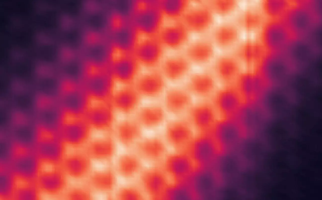
The chiral interface state, which prevents electrons from scattering backward and causing energy-wasting electrical resistance, has long been a focus of researchers in the field. Visualizing the spatial characteristics of this mysterious state has proven to be quite challenging. However, the team at Berkeley Lab and UC Berkeley has successfully captured atomic-resolution images that directly visualize the chiral interface state for the first time. This breakthrough opens up new possibilities for understanding and manipulating these resistance-free conducting channels in 2D insulators.
Experimental Breakthrough
To prepare chiral interface states, the research team created a device called twisted monolayer-bilayer graphene at Berkeley Lab’s Molecular Foundry. These stacked layers of graphene, rotated precisely relative to each other, form a moiré superlattice that exhibits the quantum anomalous Hall (QAH) effect. Using a scanning tunneling microscope at the UC Berkeley Department of Physics, the researchers were able to detect different electronic states in the sample and visualize the wavefunction of the chiral interface state.
The ability to manipulate and control chiral interface states opens up exciting possibilities for the future of quantum computing and energy-efficient electronics. By modulating the voltage on a gate electrode underneath the graphene layers, the researchers were able to move the chiral interface state across the sample. Additionally, they demonstrated that a voltage pulse from an STM probe could “write” a chiral interface state into the sample, erase it, and even rewrite a new one with electrons flowing in the opposite direction.
The findings of this research hold immense potential for the development of tunable networks of electron channels, which could pave the way for energy-efficient microelectronics and low-power magnetic memory devices. Furthermore, the exotic electron behaviors observed in QAH insulators could play a crucial role in advancing quantum computation. The researchers are eager to explore the possibilities of studying more exotic physics in related materials, such as anyons, which could hold the key to unlocking the full potential of quantum computation.
The research conducted by the international team led by Lawrence Berkeley National Laboratory marks a significant milestone in the field of quantum computing and energy-efficient electronics. The visualization and control of chiral interface states represent a major breakthrough that could shape the future of technology. With further exploration and experimentation, researchers can unlock the full potential of these exotic quantum phenomena, paving the way for a new era of innovation in quantum computing and energy-efficient electronics.


Leave a Reply