
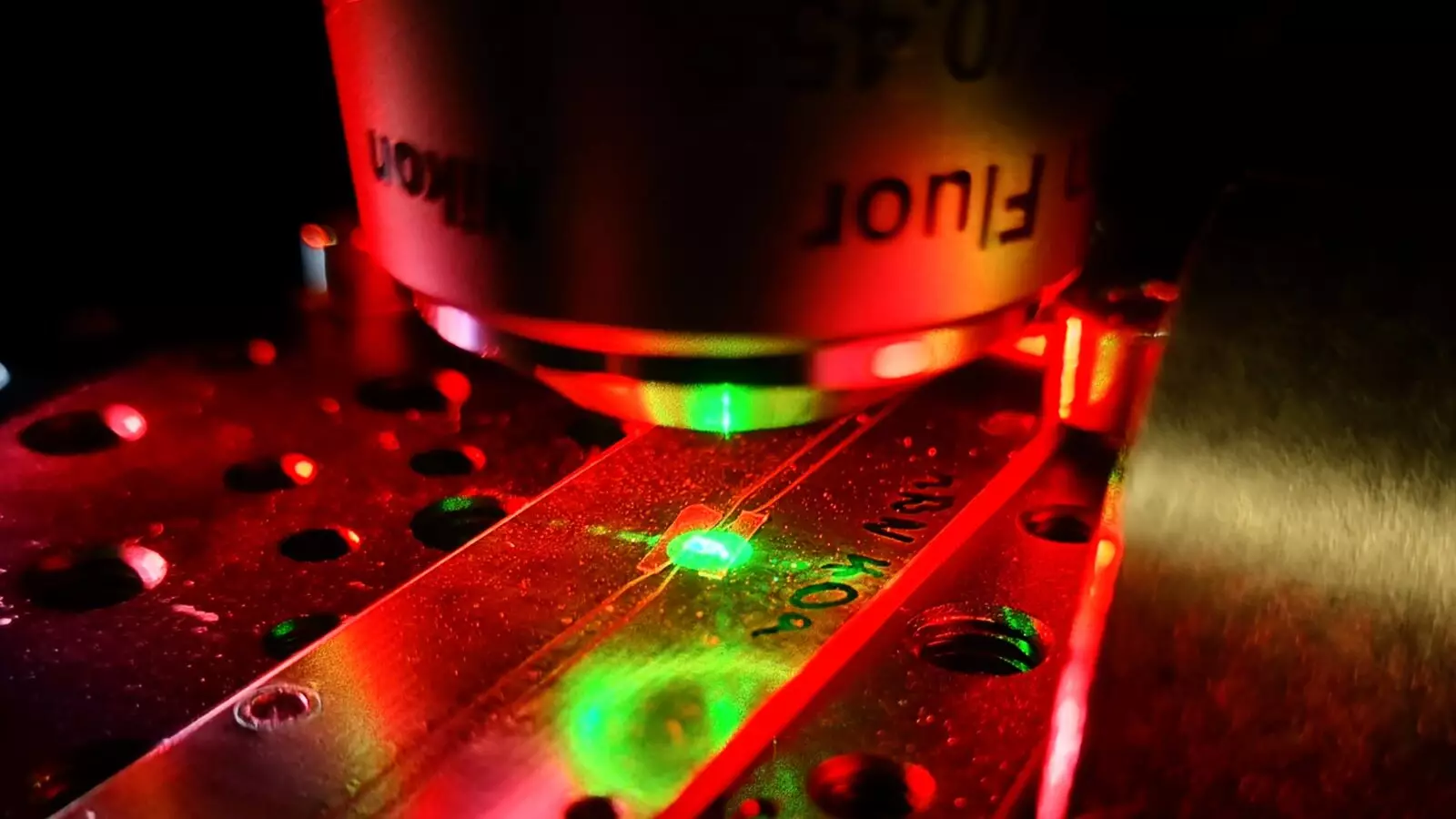
In a recent breakthrough, researchers at TMOS, the ARC Center of Excellence for Transformative Meta-Optical Systems, in collaboration with RMIT University, have introduced a new 2D quantum sensing chip utilizing hexagonal boron nitride (hBN). This innovative chip has the capability to detect temperature anomalies and magnetic fields in any direction, opening up possibilities for more versatile and cost-effective quantum sensors.
Traditionally, quantum sensing chips have been constructed from diamond due to its robust nature. However, diamond-based sensors face limitations when it comes to detecting magnetic fields in various orientations. These sensors must be aligned with the direction of the field, leading to blind spots when unaligned. As a result, diamond magnetometers require multiple sensors at different alignments, making operation more complex and limiting their versatility across different applications.
Researchers led by TMOS Associate Investigator Jean-Philippe Tetienne and Chief Investigator Igor Aharonovich are pioneering a new quantum sensing platform using hBN crystals. Unlike diamond, hBN consists of atomically thin layers that are flexible, allowing the sensing chips to conform to the shape of the sample under study. This flexibility enables the sensors to get closer to the sample, overcoming a limitation of diamond-based sensors.
Within the hBN crystals, a carbon-based defect with an unidentified atomic structure has been discovered. This defect exhibits the unique ability to detect magnetic fields in any direction, a feature that was previously untapped in magnetic imaging applications. Through a Rabi measurement experiment, researchers determined that this defect behaves as a spin half system, enabling it to sense magnetic fields omnidirectionally.
The research team showcased a hBN sensing chip that utilizes both the carbon-based half spin sensor and the well-understood boron vacancy defect simultaneously to measure magnetic field and temperature. This groundbreaking approach resulted in the first magnetic images captured with the unidentified isotropic sensor, demonstrating the potential of this new quantum sensing technology.
Compared to diamond, hBN offers several advantages in quantum sensing applications. Its 2D form factor allows for closer proximity to samples, enhancing sensing capabilities. Additionally, hBN operates as a quantum light source for communications and sensing at room temperature, eliminating the need for cryogenic cooling required by diamond. Moreover, hBN is more cost-effective and accessible, making it a promising material for future quantum sensing technologies.
The utilization of low-dimensional materials like hBN opens up possibilities for new physics discoveries due to their extreme anisotropy. Potential applications of this quantum sensing technology include in-field identification of magnetic geological features and radio spectroscopy across a wider spectrum. The continuous exploration of atomic defects in hBN will drive the development of optimized sensor devices for diverse applications, paving the way for further advancements in quantum sensing technology.
The development of a 2D quantum sensing chip utilizing hBN represents a significant milestone in the field of quantum technology. By harnessing the unique properties of this material, researchers are pushing the boundaries of quantum sensing capabilities, laying the foundation for innovative applications in various industries.
Leave a Reply