
Advancements in technology have led to the development of miniaturized optoelectronic devices that are efficient in performance and energy consumption. In recent research conducted by scientists at Fudan University, a breakthrough in integrating insulating materials with high dielectric constants into 2D semiconductors has been achieved. This new discovery could revolutionize the future of optoelectronic devices.
One of the key challenges faced in the development of miniaturized optoelectronic devices is the need for higher gate capacitance to ensure optimal performance while consuming less energy. Traditional approaches have focused on using insulating materials with high dielectric constants, such as hafnium oxide, to boost gate capacitance. However, integrating these materials with 2D semiconductors has proven to be difficult due to compatibility issues.
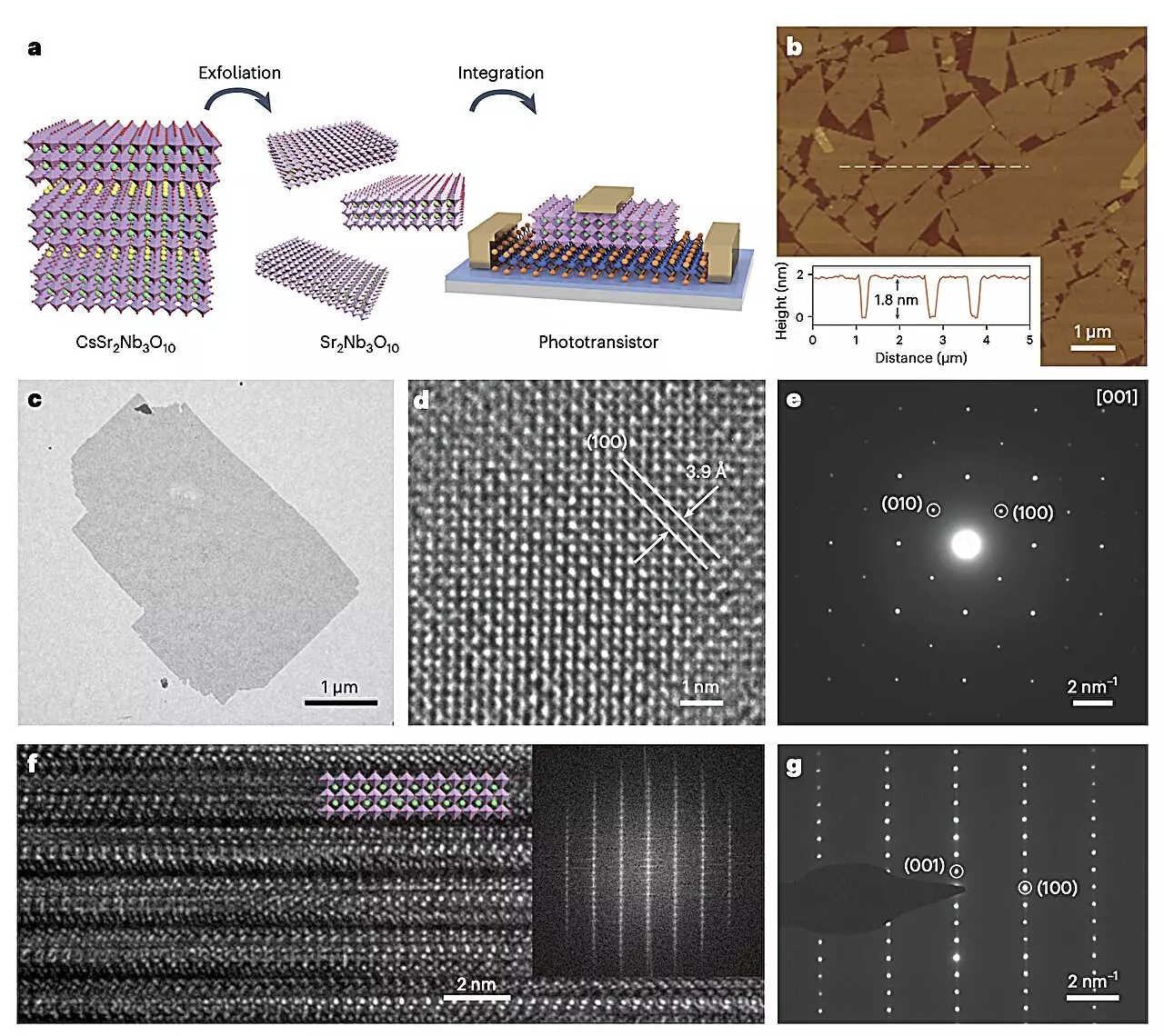
In their recent paper published in Nature Electronics, researchers introduced a 2D perovskite oxide, Sr2Nb3O10, with a high dielectric constant that can be integrated with various 2D channel materials. The synthesis of Sr2Nb3O10 using a top-down approach enabled the successful transfer of the material onto different 2D semiconductors. With a high dielectric constant of 24.6 and a moderate bandgap, Sr2Nb3O10 showed promise as a photoactive high-k dielectric for phototransistors based on graphene, molybdenum disulfide, tungsten disulfide, and tungsten diselenide.
The researchers tested the performance of transistors integrating Sr2Nb3O10 with channel materials like molybdenum disulfide and tungsten disulfide. The results were promising, with molybdenum disulfide transistors showcasing an on/off ratio of 106 and a subthreshold swing of 88mV/dec with a supply voltage of 2V. Tungsten disulfide phototransistors exhibited a photocurrent-to-dark-current ratio of ~106 and UV responsivity of 5.5 x 10³ A/W under visible or UV light illumination.
The successful integration of Sr2Nb3O10 with various channel materials demonstrates the potential for developing miniaturized optoelectronic devices with enhanced performance. The well-defined interface between the semiconductor and dielectric, combined with the high dielectric constant of Sr2Nb3O10, enables efficient gate control of channel materials. Furthermore, the researchers suggest that the use of 2D perovskite oxides could lead to the synthesis of new materials for future optoelectronic applications.
The groundbreaking research by Li, Liu, and their collaborators at Fudan University opens up new opportunities for the future of optoelectronics. The successful integration of 2D perovskite oxides with existing semiconductors and channel materials could pave the way for the development of smaller, better-performing, and energy-efficient electronics. This research marks a significant advancement in the field of miniaturized optoelectronic devices and holds great promise for the future of technology.
Leave a Reply